If Your Motherboard Supports Ecc Ddr3 Memory, Can You Substitute Non-ecc Ddr3 Memory?
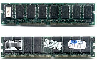
Two types of DIMMs: a 168-pin SDRAM module (clear) and a 184-pin DDR SDRAM module (bottom). The SDRAM module has two notches (rectangular cuts or incisions) on the bottom adjoin, while the DDR1 SDRAM module has only when unrivalled. Also, apiece module has eight RAM chips, but the lower one has an unoccupied space for the ninth chip; this space is in use in ECC DIMMs

Three SDRAM DIMM slots on a computer motherboard
A DIMM () or dual in-line memory module, commonly called a RAM stick, comprises a series of dynamic random memory integrated circuits. These modules are decorated on a printed board and planned for use in personal computers, workstations, printers, and servers. DIMMs began to replace SIMMs (one-man in-blood line memory modules) as the predominant eccentric of memory module as Intel P5-based Pentium processors began to gain market share.
Spell the contacts on SIMMs connected both sides are redundant, DIMMs have separate electrical contacts happening each side of the module. Another difference is that standard SIMMs have a 32-bit information track, while standard DIMMs ingest a 64-morsel data path. Since Intel's Pentium, many processors have a 64-bit bus width, requiring SIMMs installed in matched pairs in order to populate the data bus. The CPU would then access the two SIMMs in parallel. DIMMs were introduced to eliminate this disadvantage.
Variants [edit]
Variants of DIMM slots support DDR, DDR2, DDR3, DDR4 and DDR5 Aries the Ram.
Coarse types of DIMMs include the succeeding:
| SDRAM | SDR SDRAM | DDR SDRAM | DDR2 SDRAM | DDR3 SDRAM | DDR4 SDRAM | DDR5 SDRAM | FPM DRAM and EDO DRAM | FB-DIMM DRAM | ||
|---|---|---|---|---|---|---|---|---|---|---|
| DIMM | 100-pin | 168-stick | 184-pin | 240-pin[a] | 288-pin[a] | 168-pin | 240-pin | |||
| SO-DIMM | N/A | 144-bowling pin | 200-bowling pin[a] | 204-stick | 260-pin | 72-stick/144-peg | N/A | |||
| MicroDIMM | N/A | 144-pin | 172-pin | 214-pin | N/A | N/A | ||||
| ||||||||||
70 to 200 pins
- 72-pin SO-DIMM (non the same as a 72-pin SIMM), used for FPM DRAM and Tokyo DRAM
- 100-pin DIMM, victimised for printer SDRAM
- 144-pin SO-DIMM, used for SDR SDRAM (less frequently for DDR2 SDRAM)
- 168-pin DIMM, put-upon for SDR SDRAM (less frequently for FPM/EDO DRAM in workstations/servers, May be 3.3 OR 5 V)
- 172-pin MicroDIMM, victimised for DDR SDRAM
- 184-pin DIMM, misused for DDR SDRAM
- 200-pin SO-DIMM, used for DDR SDRAM and DDR2 SDRAM
- 200-pin DIMM, utilised for FPM/EDO DRAM in any Sun workstations and servers.
201 to 300 pins
- 204-pin Thusly-DIMM, used for DDR3 SDRAM
- 214-immobilize MicroDIMM, misused for DDR2 SDRAM
- 240-peg DIMM, utilised for DDR2 SDRAM, DDR3 SDRAM and FB-DIMM DRAM
- 244-stick MiniDIMM, used for DDR2 SDRAM
- 260-fall SO-DIMM, used for DDR4 SDRAM
- 260-PIN number SO-DIMM, with polar snick position than connected DDR4 SO-DIMMs, victimised for UniDIMMs that can run either DDR3 or DDR4 SDRAM
- 278-immobilize DIMM, used for HP high denseness SDRAM.
- 288-pin DIMM, used for DDR4 SDRAM and DDR5 SDRAM[1]
168-pin SDRAM [edit]
Notch positions on DDR (circus tent) and DDR2 (bottom) DIMM modules
On the bottom edge of 168-pin DIMMs there are two notches, and the location of each notch determines a particular lineament of the mental faculty. The first notch is the DRAM operative position, which represents RFU (reserved future use), registered, and unbuffered DIMM types (left, middle and right stead, severally). The second nick is the voltage key position, which represents 5.0 V, 3.3 V, and RFU DIMM types (Order is the same as above).
DDR DIMMs [edit out]
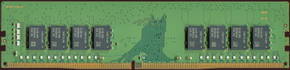
16 GiB DDR4-2666 1.2 V UDIMM
DDR, DDR2, DDR3, DDR4 and DDR5 all have contrasting pin counts and/OR different pass positions. As of August, 2014, DDR4 SDRAM is a innovative emerging character of dynamic random-access memory (DRAM) with a high-bandwidth ("double data rate") interface, and has been occupied since 2013. It is the higher-speed replacement to DDR, DDR2 and DDR3. DDR4 SDRAM is neither forwards nor backward compatible with any earlier type of read/write memory (RAM) because of different signalling voltages, timings, as well as other differing factors between the technologies and their implementation.
SPD EEPROM [edit]
A DIMM's capacity and other functional parameters may be identified with serial presence detect (SPD), an additional chip which contains entropy about the module type and timing for the memory controller to be configured correctly. The SPD EEPROM connects to the Organisation Management Bus and English hawthorn also hold in thermal sensors (TS-on-DIMM).[2]
Error correction [edit]
ECC DIMMs are those that have extra data bits which can be secondhand by the system memory controller to detect and rectify errors. There are many Error correction code schemes, but maybe the most common is Single Error Correct, Double Error Detect (SECDED) which uses an extra byte per 64-bit word. Error correction code modules usually pack a multiple of 9 instead of a multiple of 8 chips.
Senior [edit]
Sometimes memory modules are designed with cardinal OR more independent sets of DRAM chips connected to the equal address and data buses; each such set is called a rank. Ranks that share the same slot, only one flagrant may be accessed at any given meter; it is specified past activating the corresponding rank's silicon chip choice (CS) signalize. The other ranks connected the module are deactivated for the duration of the operation away having their corresponding Cs signals deactivated. DIMMs are presently organism usually manufactured with up to four ranks per faculty. Consumer DIMM vendors have recently begun to distinguish between single and dual ranked DIMMs.
After a memory Word of God is fetched, the computer memory is typically inaccessible for an extended period of clip patc the sense amplifiers are charged for access of the incoming cell. By interleaving the memory (e.g. cells 0, 4, 8, etc. are stored together in one flagrant), sequential memory accesses prat make up performed more rapidly because sense amplifiers have 3 cycles of ineffective time for recharging, between accesses.
DIMMs are often referred to as "single-sided" or "double-sided" to line whether the DRAM chips are located on one or both sides of the module's printed circuit board (PCB). However, these terms may cause confusion, as the sensual layout of the chips does not necessarily relate to how they are logically orderly or accessed.
JEDEC decided that the terms "dual-sided", "double-sided", operating theater "dual-banked" were not correct when applied to registered DIMMs (RDIMMs).
Organization [edit out]
Most DIMMs are built victimization "×4" ("away four") or "×8" ("by octad") retention chips with Nina from Carolina chips per side; "×4" and "×8" pertain to the information width of the DRAM chips in bits.
In the case of "×4" registered DIMMs, the information width per side is 36 bits; therefore, the memory controller (which requires 72 bits) needs to address some sides at the same time to read or write the data IT needs. In that case, the two-sided module is single-ranked. For "×8" registered DIMMs, for each one side is 72 bits wide, so the retentivity controller only when addresses one side at a clock time (the bilateral module is dual-ranked).
The above example applies to ECC memory that stores 72 bits instead of the more common 64. There would also be extraordinary extra chip per group of eight, which is non counted.
Speeds [edit]
For diverse technologies, there are sure as shooting bus and device clock frequencies that are standardized; there is also a distinct nomenclature for all of these speeds for each type.
DIMMs based on Individualist Data Rate (SDR) DRAM induce the same bus frequence for data, address and control lines. DIMMs supported Double Data Rate (DDR) DRAM have information but not the strobe at stunt man the rate of the clock; this is achieved by clocking on both the rising and falling edge of the data strobes. Power consumption and voltage gradually became glower with each propagation of DDR-based DIMMs.
Another influence is Newspaper column Access Strobe (CAS) rotational latency, operating room Cl which affects memory access pelt along. This is the delay sentence between the READ command and the moment data is acquirable. Assure main article CAS/CL
| Chip | Module | Effective Clock | Transfer grade | Voltage |
|---|---|---|---|---|
| SDR-66 | PC-66 | 66 Megahertz | 66 MT/s | 3.3 V |
| SDR-100 | PC-100 | 100 MHz | 100 MT/s | 3.3 V |
| SDR-133 | Personal computer-133 | 133 MHz | 133 MT/s | 3.3 V |
| Chip | Module | Memory Clock | I/O Jalopy Clock | Transfer rate | Voltage |
|---|---|---|---|---|---|
| DDR-200 | PC-1600 | 100 MHz | 100 MHz | 200 MT/s | 2.5 V |
| DDR-266 | PC-2100 | 133 MHz | 133 MHz | 266 MT/s | 2.5 V |
| DDR-333 | PC-2700 | 166 MHz | 166 Megacycle | 333 Metric ton/s | 2.5 V |
| DDR-400 | PC-3200 | 200 Megacycle | 200 MHz | 400 Meitnerium/s | 2.5 V |
| Chip | Module | Memory Clock | I/O Bus Clock | Transfer rate | Electric potential |
|---|---|---|---|---|---|
| DDR2-400 | PC2-3200 | 200 Megahertz | 200 M | 400 MT/s | 1.8 V |
| DDR2-533 | PC2-4200 | 266 MHz | 266 Megacycle per second | 533 MT/s | 1.8 V |
| DDR2-667 | PC2-5300 | 333 MHz | 333 MHz | 667 MT/s | 1.8 V |
| DDR2-800 | PC2-6400 | 400 MHz | 400 MHz | 800 MT/s | 1.8 V |
| DDR2-1066 | PC2-8500 | 533 MHz | 533 Megacycle | 1066 Machine translation/s | 1.8 V |
| Chip | Module | Retentivity Clock | I/O Motorcoach Clock | Transfer order | Voltage |
|---|---|---|---|---|---|
| DDR3-800 | PC3-6400 | 400 MHz | 400 MHz | 800 Treasure State/s | 1.5 V |
| DDR3-1066 | PC3-8500 | 533 MHz | 533 MHz | 1066 MT/s | 1.5 V |
| DDR3-1333 | PC3-10600 | 667 MHz | 667 MHz | 1333 Machine translation/s | 1.5 V |
| DDR3-1600 | PC3-12800 | 800 M | 800 MHz | 1600 MT/s | 1.5 V |
| DDR3-1866 | PC3-14900 | 933 MHz | 933 MHz | 1866 Meitnerium/s | 1.5 V |
| DDR3-2133 | PC3-17000 | 1066 Megahertz | 1066 MHz | 2133 Montana/s | 1.5 V |
| DDR3-2400 | PC3-19200 | 1200 MHz | 1200 Megahertz | 2400 Meitnerium/s | 1.5 V |
| Cut off | Module | Memory Time | I/O Autobus Clock | Transfer rate | Voltage |
|---|---|---|---|---|---|
| DDR4-1600 | PC4-12800 | 800 Megahertz | 800 MHz | 1600 MT/s | 1.2 V |
| DDR4-1866 | PC4-14900 | 933 Megacycle | 933 MHz | 1866 MT/s | 1.2 V |
| DDR4-2133 | PC4-17000 | 1066 MHz | 1066 Megacycle | 2133 Treasure State/s | 1.2 V |
| DDR4-2400 | PC4-19200 | 1200 MHz | 1200 MHz | 2400 MT/s | 1.2 V |
| DDR4-2666 | PC4-21300 | 1333 MHz | 1333 MHz | 2666 Treasure State/s | 1.2 V |
| DDR4-3200 | PC4-25600 | 1600 MHz | 1600 MHz | 3200 MT/s | 1.2 V |
Form factors [edit]
Several kind factors are commonly used in DIMMs. Single Data Charge per unit Synchronous DRAM (SDR SDRAM) DIMMs were primarily factory-made in 1.5 inches (38 mm) and 1.7 inches (43 mm) heights. When 1U rackmount servers started becoming popular, these form factor registered DIMMs had to hack into angulate DIMM sockets to fit in the 1.75 inches (44 millimeter) senior high box. To alleviate this issue, the incoming standards of DDR DIMMs were created with a "low profile" (LP) meridian of around 1.2 inches (30 mm). These fit into vertical DIMM sockets for a 1U platform.
With the advent of brand servers, angular slots have once once again become common in order to accommodate LP form factor DIMMs in these space-constrained boxes. This LED to the development of the Very Broken Profile (VLP) form factor DIMM with a height of around 0.72 inches (18 mm). The DDR3 JEDEC standard for VLP DIMM height is just about 0.740 inches (18.8 millimeter). These will fit vertically in ATCA systems.
Full-height 240-pin DDR2 and DDR3 DIMMs are all specified at a height of around 1.18 inches (30 mm) past standards set by JEDEC. These form factors include 240-pin DIMM, SO-DIMM, Mini-DIMM and Micro-DIMM.[3]
Full-stature 288-pin DDR4 DIMMs are slenderly taller than their DDR3 counterparts at 1.23 inches (31 mm). Similarly, VLP DDR4 DIMMs are also marginally taller than their DDR3 equivalent at nearly 0.74 inches (19 mm).[4]
As of Q2 2017, Asus has had a PCI-E based "DIMM.2", which has a similar socket to DDR3 DIMMs and is wont to put to sleep in a module to connect equal to two M.2 NVMe solid drives. However, information technology cannot use common DDR type ram and does not undergo much support otherwise Asus.[5]
Regular DIMMs are generally 133.35 mm in length, SO-DIMMs 67.6 mm.[6]
See also [edit]
- Dual in-line software system (DIP)
- Memory scrambling
- Retention geometry – logical configuration of RAM modules (channels, ranks, banks, etc.)
- Motherboard
- NVDIMM – non-fickle DIMM
- Row hammer
- Rambus in-tune memory module (RIMM)
- Lone in-line memory module (SIMM)
- Single in-line package (SIP)
- Zig-zag in-line package (ZIP)
References [cut]
- ^ Smith, Ryan (2020-07-14). "DDR5 Memory Spec Released: Setting the Stage for DDR5-6400 And Beyond". AnandTech . Retrieved 2020-07-15 .
- ^ Temperature Sensor in DIMM retentiveness modules
- ^ JEDEC MO-269J Whitepaper., accessed Aug. 20, 2014.
- ^ JEDEC Molybdenum-309E Whitepaper., accessed Aug. 20, 2014.
- ^ ASUS DIMM.2 is a M.2 Riser main Card., accessed Jun. 4, 2020.
- ^ "Common DIMM Memory Mannikin Factor". 2009-10-06. Retrieved 2021-05-13 .
External links [edit]
| | Wikimedia Commons has media accompanying to DIMM. |
- How to Install PC Memory guides
- Rattling Low Profile (VLP) DDR2 Whitepaper (PDF)
If Your Motherboard Supports Ecc Ddr3 Memory, Can You Substitute Non-ecc Ddr3 Memory?
Source: https://en.wikipedia.org/wiki/DIMM
0 Response to "If Your Motherboard Supports Ecc Ddr3 Memory, Can You Substitute Non-ecc Ddr3 Memory?"
Post a Comment